Sketch The I-v Characteristics Of An Ideal Rectification Diode.
Onlines
Mar 16, 2025 · 5 min read
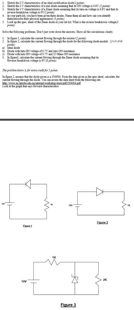
Table of Contents
Sketching the I-V Characteristics of an Ideal Rectification Diode
The ideal rectification diode, a cornerstone component in electronics, forms the basis for understanding more complex diode behaviors. While real-world diodes exhibit non-ideal characteristics, mastering the ideal model is crucial for circuit analysis and design. This article provides a comprehensive guide to sketching the I-V characteristics of an ideal diode, exploring its key properties and implications in various applications.
Understanding the Ideal Diode Model
The ideal diode is a simplified representation that behaves as a perfect one-way valve for current. Its behavior can be summarized by two distinct states:
1. Forward Bias:
When a positive voltage (V) is applied across the diode's anode (positive terminal) with respect to its cathode (negative terminal), the diode acts as a closed switch, offering almost zero resistance to the flow of current (I). This means current flows freely, and the voltage drop across the diode is considered negligible (approximately 0V).
2. Reverse Bias:
When a negative voltage (V) is applied, with the cathode at a higher potential than the anode, the diode behaves as an open switch, offering infinite resistance. No current (I) flows through the diode, regardless of the magnitude of the reverse bias voltage.
Sketching the I-V Curve: A Step-by-Step Approach
To sketch the I-V characteristics of an ideal diode, we plot the current (I) on the vertical axis (y-axis) and the voltage (V) on the horizontal axis (x-axis). The resulting curve is remarkably simple due to the diode's binary behavior:
-
The Forward Bias Region (V > 0): In this region, the ideal diode acts as a short circuit. This translates to a vertical line originating from the origin (0,0) and extending infinitely upwards along the positive y-axis. This indicates that any positive voltage will result in an infinitely large current flow. This is, of course, a theoretical limit. In reality, the diode's forward current is limited by external circuit elements.
-
The Reverse Bias Region (V < 0): Here, the diode behaves as an open circuit. This is represented by a horizontal line along the negative x-axis, indicating zero current flow regardless of the negative voltage applied. The line extends infinitely to the left, showing that the diode blocks current even under large reverse bias voltages.
Visual Representation:
Imagine a graph. The x-axis represents the voltage (V) applied across the diode, and the y-axis represents the current (I) flowing through it.
-
Positive x-axis (V > 0): A vertical line along the positive y-axis from the origin. This represents the near-zero resistance in the forward bias.
-
Negative x-axis (V < 0): A horizontal line along the negative x-axis. This represents the infinite resistance in the reverse bias.
This simple graph clearly illustrates the "on" and "off" behavior of the ideal diode. There's a sharp transition between these two states at V=0.
Comparing Ideal and Real Diodes: Understanding the Discrepancies
While the ideal diode model simplifies analysis, real diodes deviate significantly. Several factors contribute to this divergence:
1. Forward Voltage Drop:
Real diodes require a minimum voltage, known as the forward voltage drop (V<sub>f</sub>), before they start conducting significantly. This voltage drop is typically around 0.7V for silicon diodes and 0.3V for germanium diodes. The I-V curve for a real diode starts not at the origin but at a point (V<sub>f</sub>, 0).
2. Reverse Saturation Current:
Contrary to the ideal model, real diodes allow a small reverse saturation current to flow even under reverse bias. This current is extremely small but not zero. This is due to minority carriers in the semiconductor material.
3. Breakdown Voltage:
Applying a sufficiently large reverse voltage will cause a real diode to enter the breakdown region. Here, the reverse current increases dramatically, potentially damaging the diode. This is not represented in the ideal diode model.
4. Non-linearity:
The current-voltage relationship in a real diode is not perfectly linear in the forward bias region. The current increases exponentially with the voltage above the forward voltage drop.
Applications of Ideal Diode Characteristics: A Glimpse into Practical Scenarios
The understanding of the ideal diode's I-V characteristic is fundamental to analyzing and designing many electronic circuits.
1. Rectification:
The most prominent application is rectification, converting alternating current (AC) to direct current (DC). The ideal diode's one-way conduction allows only positive half-cycles of the AC signal to pass, creating a pulsating DC output. Analyzing the output waveform requires considering the ideal diode’s I-V relationship.
2. Clipping and Clamping Circuits:
Ideal diodes are crucial in clipping and clamping circuits that shape waveforms by selectively removing portions of the signal or shifting its DC level. The diode's sharp switching action (ideal model) is essential for precise waveform modification.
3. Logic Gates:
Simplified logic gates such as AND, OR, and NOT gates can be implemented using ideal diodes in conjunction with resistors. The diodes' binary behavior mirrors the logic operations directly.
4. Switching Circuits:
High-speed switching operations often utilize the fast switching characteristics of diodes, especially in power electronics. Model simplification through the ideal diode approximation facilitates initial circuit design and analysis.
5. Diode ORing:
In power systems and instrumentation, multiple power sources can be connected to a single load using diode ORing. Each diode ensures that only the active source powers the load; the others remain idle. The ideal diode's characteristic simplifies the circuit analysis.
Conclusion: Bridging Theory and Practice
The I-V characteristic of an ideal diode, though a simplification, provides a strong foundation for understanding diode operation. While real diodes deviate from this ideal model, mastering the basics is essential. By visualizing the idealized I-V curve—a vertical line in the forward bias region and a horizontal line in the reverse bias region—you build the crucial understanding needed to tackle the complexities of real-world diode behavior and its numerous applications in diverse electronic circuits. Remember, the ideal model is an invaluable tool for initial circuit analysis, providing a starting point for more refined modeling that incorporates non-ideal characteristics when necessary for higher accuracy. This approach combines the elegance of theoretical simplification with the practical realities of circuit design and analysis.
Latest Posts
Latest Posts
-
What Is The Final Product Of An Operational Design
Mar 17, 2025
-
Thinking Fast And Slow Chapter Summary
Mar 17, 2025
-
Skills Module 3 0 Maternal Newborn Posttest
Mar 17, 2025
-
Which Statements Correctly Describe Licensing Agreements
Mar 17, 2025
-
Rn Maternal Newborn Teaching Prenatal And Newborn Care
Mar 17, 2025
Related Post
Thank you for visiting our website which covers about Sketch The I-v Characteristics Of An Ideal Rectification Diode. . We hope the information provided has been useful to you. Feel free to contact us if you have any questions or need further assistance. See you next time and don't miss to bookmark.
